Synthetic carbon allotropes
Carbon occurs naturally in a number of different forms, or “allotropes”, with graphite and diamond being the most common ones. Various new, synthetic carbon allotropes have been developed in the last decades. Graphene is possibly the most famous one and has been in the focus of our research. We plan to extend our investigations to novel synthetic carbon allotropes like graphene nanoribbons and related systems with extended electronic pi-systems, or to diamandoids, which are nanometer-sized sp3 hybridized systems.

On many metal surfaces graphene can be grown (almost) perfectly as a single layer by thermal decomposition of simple hydrocarbons at the surface. Alternatively, extremely well-ordered layers of graphene form on SiC during thermal decomposition.
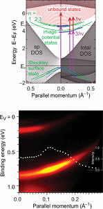
We investigate the structural properties of the graphene-metal interface by LEED and STM. We further look into the electronic interactions between the graphene and the supporting substrate using photoelectron spectroscopy and time-resolved two-photon photoelectron spectroscopy. This allows to determine the electron transfer times between graphene and the substrate on the femtosecond time scale.
Publications
- Gugel, Dieter, et al. "Two-photon photoemission from image-potential states of epitaxial graphene." 2D Materials 2.4 (2015): 045001.
- De Andres, P. L., et al. "One-dimensional potential for image-potential states on graphene." New Journal of Physics 16 (2014).
- Niesner, Daniel, and Thomas Fauster. "Image-potential states and work function of graphene." Journal of Physics: Condensed Matter 26 (2014).
- Nobis, David, et al. "Image-potential states of graphene on noble-metal surfaces." Physical Review B 88 (2013).
- Niesner, Daniel, et al. "Trapping surface electrons on graphene layers and islands." Physical Review B 85 (2012).

One of the most important proplems to be tackled before using graphene in electronic devices is how to contact graphene by (metal) thin film contats. We use STM and STS to investigate the binding, electron transfer and modification of substrate coupling between different metals and epitaxial graphene layers grown on SiC.
While graphene seems a perfect two-dimensional conductor there are inevitably defects that arise from the interaction between the graphene layer(s) and the substrate. In this project we employed Scanning Tunneling Potentiometry to delineate the potential drop at atomic scale defects like substrate steps, monolayer-bilayer junctions or wrinkles of the graphene layer.
This project was supported by the Deutsche Forschungsgemeinschaft within the priority programme SPP 1459 “Graphene”.
Publications
- Sokolova, Anastasia, et al. "Sub-Monolayer Growth of Titanium, Cobalt, and Palladium on Epitaxial Graphene." Annalen Der Physik 529.11 (2017).
- Willke, P., M. Alexander Schneider, and M. Wenderoth. "Electronic Transport Properties of 1D-Defects in Graphene and Other 2D-Systems." Annalen Der Physik 529.11 (2017).
- Willke, Philip, et al. "Spatial extent of a Landauer residual-resistivity dipole in graphene quantified by scanning tunnelling potentiometry." Nature Communications 6 (2015).
